ASML、チップ露光装置から先進パッケージング事業へ拡大を計画
本文の状態
日本語全文を表示中
詳細モードで約1分の本文を読めます。
同じ出来事の情報源
この情報源を基点に整理
The Decoder
ASMLは、最先端チップ製造に用いられるEUV露光装置の唯一のメーカーとして、中核事業を超えて先進パッケージング分野への拡大を目指している。
Source Article
元記事を日本語で読む
本文に関係しない購読案内、埋め込み通知、サイト内プロモーションは除いています。
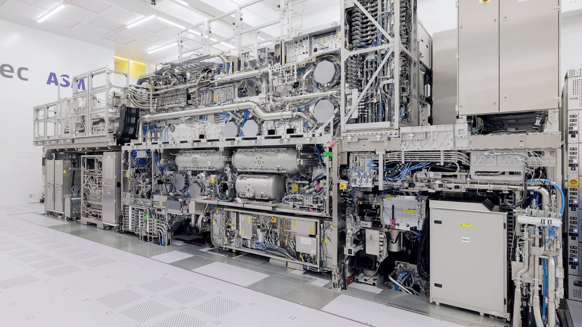
先進的チップの製造に用いられるEUV(極端紫外線)リソグラフィ装置の世界唯一のメーカーであるASMLは、中核事業の枠を超えた拡大を目指している。
本記事「ASML plans to expand beyond chip lithography into advanced packaging」は、The Decoderに最初に掲載されました。
原文を表示
ASML, the world's sole manufacturer of EUV lithography machines used to produce advanced chips, is looking to expand beyond its core business. That's according to a Reuters report citing ASML Chief Technology Officer Marco Pieters.
The Dutch company is specifically planning to move into advanced packaging - a technique where multiple specialized chips are connected and stacked on top of each other. This approach is critical for modern AI chips and the high-bandwidth memory that feeds them. TSMC already uses advanced packaging to build Nvidia's most powerful AI processors, among others.
Pieters told Reuters that ASML is planning 10 to 15 years ahead, studying what kinds of machines the industry will need for packaging and bonding. The company is also exploring whether chips can be printed beyond their current size limit. On top of that, ASML wants to use AI to speed up the control software running its machines and improve quality checks during chip manufacturing.
AI News Without the Hype – Curated by Humans
Subscribe to THE DECODER for ad-free reading, a weekly AI newsletter, our exclusive "AI Radar" frontier report six times a year, full archive access, and access to our comment section.
今日のまとめ
AIデイリーブリーフで今日の重要ニュースをまとめ読み