Llama 3.1 8B をシリコンに刻印する新興企業 Taalas の挑戦と市場の警戒
本文の状態
日本語全文を表示中
詳細モードで約23分の本文を読めます。
同じ出来事の情報源
この情報源を基点に整理
TLDR AI
AI推論のボトルネックであるメモリ帯域壁を突破するため、モデル重みを物理的にシリコンに刻み込むASIC化が加速しており、これが業界のパラダイムシフトを招いている。
Continue in AI NEW LAB
このニュースを、実務の判断につなげる
AI NEW LABで、試したことや先に確認したい条件を共有できます。まずはログインなしで読めます。
AI NEW LABで論点を見るAI深層分析を開く2026年8月11日 22:31
AI深層分析
キーポイント
ASIC によるモデルの物理的固定化
Taalas は Llama 3.1 8B の重みをメモリに読み込むのではなく、ファブで物理トランジスタとして刻み込み、Groq と同様に速度向上を追求している。
メモリ帯域壁の突破
GPU は推論時に計算よりも重みの移動にエネルギーを消費するが、オンダイで重みを保持するチップは HBM を不要とし、このボトルネックを解消する。
歴史的な技術転換のパターン
ビットコイン採掘や YouTube の動画変換など、ワークロードが定着すると汎用ハードウェアから専用 ASIC へ移行し、柔軟性を効率と交換する傾向が見られる。
Nvidia と AMD の参入
Taalas や Groq のようなアプローチに対し、Nvidia と AMD が数ヶ月以内にそれぞれ対応策を講じており、業界全体がこの方向へ向かっている。
オンダイSRAMによる製造負荷の分散
重みをチップ内部のSRAMに保持する設計はHBMを不要とし、2027年に供給が逼迫しているメモリ工場の容量に依存しない。これにより推論処理を既存のGPUと組み合わせて行うことで、RAMやVRAMへの需要圧力を軽減できる。
重要な引用
Instead it was a Toronto company that had taken Llama 3.1 8B and etched it into silicon - not loaded it, etched it, the weights laid down as physical transistors at the fab.
Every previous time a workload left general-purpose hardware, it permanently changed who could afford to run it
A chip that holds its weights on-die needs no HBM at all.
On a GPU the weights make the trip, on the specialized chips the data does.
編集コメントを表示
編集コメント
モデルの重みを物理的に固定するアプローチは、柔軟性の犠牲を払うことで極限の速度を実現する戦略であり、業界全体のインフラ設計を根本から変える可能性を秘めている。この動きは単なるハードウェアの進化ではなく、AI サービスのコスト構造と参入障壁そのものを再定義する転換点となるだろう。
Source Article
元記事を日本語で読む
本文に関係しない購読案内、埋め込み通知、サイト内プロモーションは除いています。
私は 2 月に初めて Taalas という企業について知りました。その時、私が開いたのは Hacker News のスレッドで、期待していたのはベンチマークチャートを持つ別の推論スタートアップの話題でした。しかし現れたのはトロントの会社であり、Llama 3.1 8B をシリコンに刻み込んだという話でした。単にロードしただけではなく、ファブ(製造工場)において重みを物理的なトランジスタとして埋め込むことで、ハードウェアレベルで定着させたのです。
私の最初の感想は「これが新しい」ということではなく、「これは以前にもあった話だ」というものでした。Groq は同じ課題を何年も追っており、一歩手前で止まっています。彼らは重みをチップ上に保持しつつも、書き換え可能な状態にしていました。両者に共通する問いはこうです。「速度と引き換えに、モデルのどの部分を永久化させる気があるのか?」。
それから 8 ヶ月もしないうちに、Nvidia はその一方を、AMD は他方を買収しました。ここが注目すべき点です。今まさにカーテンの裏側で、非常に重要なことが起こっています。しかしこれがチップ関連のニュースとして報じられるため、見過ごされがちなのです。
過去にワークロードが汎用ハードウェアから離れるたびに、それを動かせるコストを負担できる企業や組織は永久に変化しました。AI の推論も今まさにその過渡期にあります。この動きがどこまで進むかは、単に測定を待つ固定された量ではありません。なぜなら問題のあらゆる側面——モデル自体、シリコン設計、そして驚くべきことに、モデルが出力を生成する仕組みそのもの——がまだ設計段階にあるからです。
We've seen this movie
ビットコインマイニングは、4 年という短期間で CPU から GPU、FPGA、そして特定の用途に特化した ASIC(専用集積回路)へと進化しました。ASIC は一つの作業しか行わないチップです。各段階で柔軟性は犠牲になり、効率性が追求されましたが、一度進んだ道には後戻りできません。2013 年に最初の Avalon ユニットが出荷された際、GPU によるマイニングが遅くなったわけではありません。ただ、意味をなさないものになったのです。
このパターンは現在、至る所に存在します。その普及ぶりが逆に目立たないほどです。YouTube は独自の Argos チップ で動画のトランスコードを行っており、Google によればこれは以前の最適化されたソフトウェア構成よりも 20 倍から 33 倍も優れています。ネットワークスイッチングは Broadcom のシリコンが担っています。スマートフォンには H.265 デコード用の固定機能ブロックや、カメラ用の ISP(イメージ信号プロセッサ)、そして他の何もしない Secure Enclave が備わっています。これは、負荷が安定し、金属に鋳込む価値がある状態に至った時に起こる現象です。この物語もまた、その条件点で終わりを迎えます。
皆がぶつかる壁
推論(インファレンス)中に GPU がエネルギーの大部分を消費するのは、計算ではなく重み(ウェイト)の移動です。各層、各トークンにおいて、重みは HBM(GPU デイスの隣にあるスタック型 DRAM、高帯域幅メモリ)から取り出され、計算ユニットを通り抜けて次の層へと送られます。32 層のモデルでは、1 つのトークンを生成するためにこのプロセスが 32 回繰り返され、次のトークン用に最初からやり直されます。これが「メモリの壁」です。推論は計算能力ではなく帯域幅によって制限されており、HBM は AI サーバーの中で最も高価なコンポーネントなのです。
チップが重みをダイ内に保持すれば、HBM は不要です。そのメモリは SRAM であり、論理ウェーハ上に印刷されます。製造工場は、2027 年の生産量がすでに完売しているというメモリープラントの一つではありません 2027 output is already sold。つまり、推論処理をこうしたシリコンに移行することで、製造負荷がすでに確保された容量へと分散され、私たちが入手しようとしている RAM や VRAM への圧力が和らぎます。ただし、どの程度圧力を軽減できるかは未定です。なぜなら、これらのチップと組み合わされる GPU は依然として HBM を搭載しているからです。
この実現を成し遂げたのは二社ですが、それらが目指した「モデルのどこまでを凍結(固定)するか」という点で方針が分かれています。その選択が、その後のすべてを決めます。
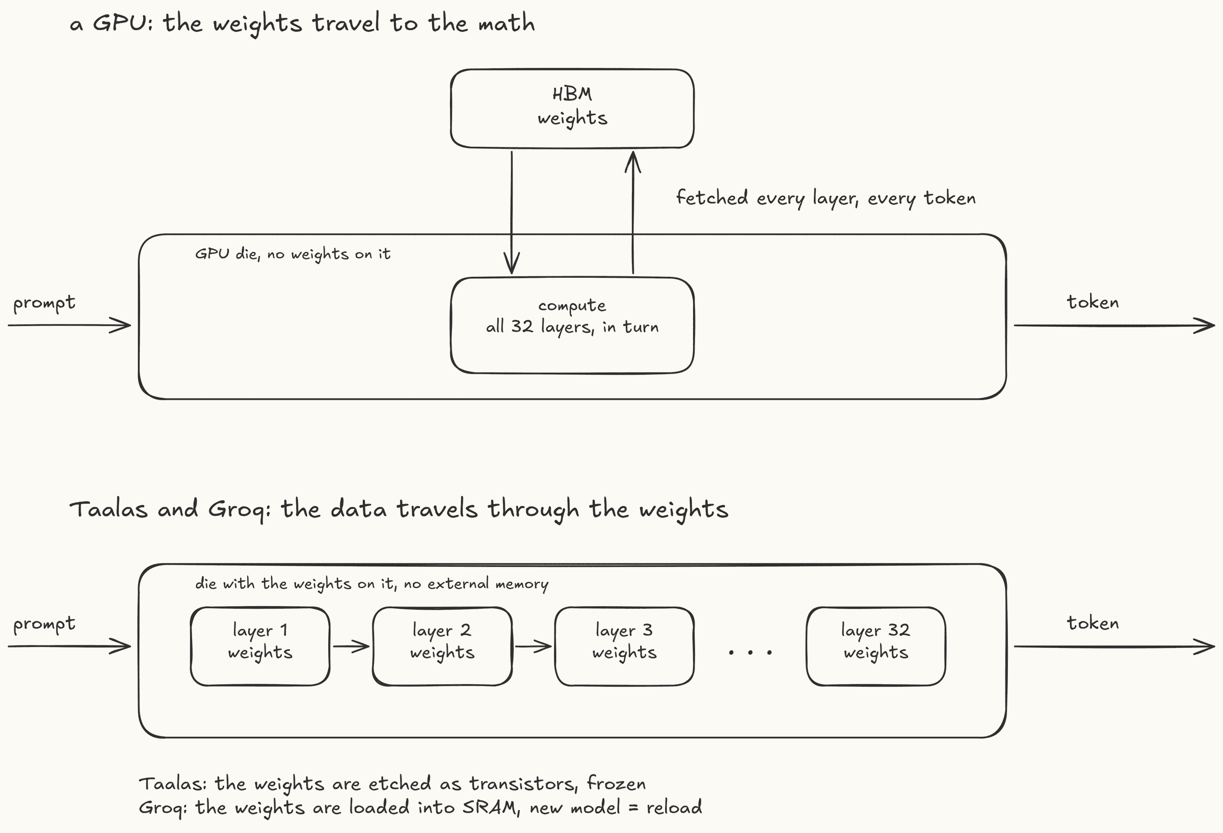
同じプロンプトからトークンへの変換処理を両方とも行います。GPU では重み(weights)が移動し、専用チップではデータが移動します。
賭け事その1:モデルこそがシリコンである
Taalas は、製造時に一度だけ書き込まれる読み取り専用メモリ(mask-ROM)である「マスク ROM ファブリック」に重みを格納します。この構造では、1 つのトランジスタが 4 ビットを保存すると同時に、それに関連する乗算演算も実行します。データはチップ内の物理層を順次流れ、外部メモリに戻ることはありません。
以下はベンダーが発表した数値です(すべて独立した検証は行われていません):
- Llama 3.1 8B でユーザーあたり 16,960 トークン/秒。これは H200 の約 230 トークン/秒と比べて桁違いです。実際に 公開デモ を体験した人からは、14,000〜17,000 トークン/秒という報告も上がっています。
- 0.015 J/token の消費電力。これは Groq が自社の数値として発表している 1〜3 と比較し、H100 クラスのシステムが EE Times の報道によると 10〜30 J/token であることと比べても圧倒的に低いです。
- 100 万トークンあたり $0.0075。一般的な価格帯である $0.20〜$0.50 と比べると非常に安価です。
- TSMC の N6 プロセスを採用し、面積は 815 mm²。トランジスタ数は 530 億個、カードあたりの消費電力は約 250 W です。この 1 チップで 8B モデル全体を収容できます。
「シリコンに刻印された」という表現は、チップがファブから出た瞬間に固定されてしまうかのように聞こえます。多くの報道や、私自身も最初はそう捉えていましたが、実際にはそう単純ではありません。
このダイ(チップ)には二つの領域があります。マスク ROM 構造体が凍結された重み(ウェイト)を保持しています。その隣には SRAM リコール構造体があり、これは同じチップ上の書き換え可能なメモリです。ここには KV キャッシュや LoRA アダプターが格納されます。LoRA アダプターは、モデルを再学習させることなく特定のドメインへ誘導するための少量の追加重みセットです。
これらはチップが動作中に切り替わります。例えば、法律用アダプターを使えば法的な言語を、臨床用アダプターを使えば医療用語を出力しますが、その背後にある「刻印された」モデル自体は同じものです。
また、凍結された部分も完全な再設計ではありません。チップは複数のパターン化された層のスタックから構成されており、各層は独自のフォトマスクを通じて印刷されます。このマスクセットを作成することが最も高価な工程であり、ウェーファーが一つ動く前に工具代として支払われるコストです。
Taalas は毎回同じ基本スタックを再利用しており、約 100 層のうち重みを担うのはわずか 2 層だけです。新しい重みから出荷可能なカードに至るまでの期間は約2 ヶ月とされています。一方、完全なカスタム設計では通常 6 ヶ月以上かかります。
コストを特定するのは難しいです。なぜなら、公開されているマスクの価格は桁違いに異なるからです。Taalas 自体に関する最も具体的な見積もりは、zach.be の記事にあるもので、DeepSeek-R1 クラスのモデル向けに約 30 種類のチップバリアントと、マスク代として1 億ドルが必要とされています。つまり、バリアントあたり約300 万ドルとなり、投資回収には 1 年間のサービス寿命が必要です。
つまり、これは二項対立ではなく連続したスペクトラムであり、300万ドルはすでに大規模推論サービスを提供している企業にとっては単なる経費項目に過ぎません。しかし、それでもなお基盤となるのはシリコンです。
2 ヶ月は設計期間であって納品までの期間ではありません。Taalas はすでに自社のスケジュールを 1 年遅らせており、その後に製造、検証、ラックからのカード交換といった工程が待っています。また、このアダプターはハードウェアに焼き付けられた重みを書き換えるのではなく、それを誘導するものです。つまり、チップは用語を受け入れることはできても、エッチングされたモデル自体には存在しない能力を獲得できるわけではありません。ベースモデルの改訂、トークナイザーの変更、あるいは新アーキテクチャの導入は、すべて新しいマスクと新しいカードを必要とします。
2 つ目の賭け:モデルはロード可能である
Groq は同じ壁に別の側面から挑みました。両社を比較すればするほど、私はこの「ヘッジ(対抗策)」こそが最も興味深い部分だと考えます。LPU(Language Processing Unit)にも HBM は搭載されていません。重みはオンチップの SRAM に配置され、すべての命令とデータ移動を事前に計算するコンパイラ によって管理されるため、実行時に決定されることは一切なく、ジョブ開始前にレイテンシが確定します。どんなモデルでもこの上で動作可能であり、切り替えには再コンパイルとロードが必要ですが、これは数分で完了し、新たなハードウェアの導入は不要です。
そのコストは、容量の問題です。第 1 世代の LPU はチップあたり 230 MB の SRAM を搭載していますが、8 ビット量化された 7B モデルを収めることさえできず、70B モデルでは 576 チップが必要になります。これには、各チップごとの相互接続、電力供給、そして設置スペースも含まれます。
LP30 ダイ は、問題の根本を解決するわけではありませんが、比率を改善しています。容量は約 500 MB に増え、ラックあたり 256 チップでオンチップ SRAM が合計 128 GB になります。それでも、Taalas が 1 つのダイに収めることができる量を保持するには、依然として数百個のチップが必要です。
彼らが実際に賭けているもの
Taalas は重み(weights)が固定されることを前提としています。つまり、モデルはマスキングのコストを回収できるだけの期間、有用であり続けるという前提です。その経済性から算出された期間は、約 1 年とされています。
一方、Groq が賭けているのはアーキテクチャのみが固定されることです。トランスフォーマー構造自体は不変ですが、内部の重みは数ヶ月ごとに更新され続けます。Taalas はモデルあたりシリコンコストが高くつき、Groq はモデル変更のたびにシリコンコストがかかります。
両方の賭けは、すでに資金によって裏付けられています。Nvidia は 12 月、Groq のアーキテクチャを 200 億ドルでライセンス契約し、AMD もそれから約 7 ヶ月後に Taalas を買収することに合意しました。これは、自社の製品が大半の処理に適さない形になることへの保険です。
どちらの取引よりも興味深いのは、両方の買い手が同じシステム設計を説明している点です。プロンプトへの回答には 2 つのフェーズがあります。1 つ目は入力を読み込むフェーズで、これは並列計算であり、GPU が得意とする処理です。2 つ目は単語を一つずつ書き出すフェーズで、次の単語に進む前にモデル全体を再使用する必要があります。
両社とも、最初のフェーズには GPU を使い、2 番目のフェーズには専用のチップを採用しています。どちらの戦略も「何を固定するか」という点では正反対ですが、労働分担の仕方は全く同じです。
アナロジーが崩れる地点
Bitcoin が ASIC を手に入れたのは、SHA-256 が仕様であり、2002 年に標準化されたからです。これは Bitcoin の誕生よりも数年も前の話です。この仕様は決して変わりません。「おそらく変わらない」のではなく、「絶対に変われない」のです。なぜなら、変更すればそれは別の通貨になってしまうからです。
動画コーデックも同じ道を進みました。フォーマットを標準化し、時間を置いてからシリコンに実装するのです。
その前提条件は「この処理負荷が人気があること」ではありませんでした。「この処理負荷が完成していること」こそが真の前提だったのです。
LLM は非常に柔軟なツールであり、まだ完成の域には達していないと考えています。Llama 3.1 8B が 2024 年 7 月に登場したことを考えると、HC1 は 2026 年 2 月に出荷される際、すでに 19 ヶ月も前のモデルをベースにしています。そのサイズクラスでは、さらに優れたモデルが既に存在しているのです。シリコンの製造には時間がかかるため、世界が次のステップへ進んだ後にようやく製品が届いてしまうというジレンマがあります。
よくある反論として「開発ペースは落ち着くだろう」というものがありますが、私は半分だけ同意します。確かに*画期的な技術革新*の速度は鈍化しているように見えます。トランスフォーマーアーキテクチャが 9 年間も支配し続けており、エキスパート混合(MoE)が標準となり、真に新しいアーキテクチャアイデアが登場する間隔も広がっています。しかし、モデルのリリース頻度が大幅に遅れることはなく、この「リリース」こそが半導体市場を揺さぶる要因です。Llama 3.1 から 3.2、そして 3.3 へ、Qwen 2.5 から 3 へと、ポストトレーニングによる刷新やトークナイザーの差し替えが行われます。これらはすべてアーキテクチャは同一のまま数値(パラメータや学習データなど)のみを変更するものであり、その「数値」こそが金属として鋳造される部分なのです。
さらに、多くの顧客にとって最も重要なのは柔軟性です。スマホのアシスタントに「請求書のこの料金は何ですか?」と尋ねると、音声認識、スクリーンショットを解析するビジョンモデル、それについて推論を行う言語モデル、そして音声合成という 4 つのモデルが連携し、3 つ異なるモダリティ(音声・画像・テキスト)を扱います。これは一つの質問に対して行われる処理ですが、より優れたモデルが登場するたびにその組み合わせは変化します。特定のタスクに極めて高速に対応できる一方で、他のタスクには全く対応できないチップでは、実用性はほとんど得られません。
誰も買おうとしていないダークホース
これまでの議論のすべてが一つの前提に基づいています。「モデルは単語を一つずつ生成する」という考え方です。両方の設計はこの前提の上に成り立っています。しかし、モデルにそれを強制するものはありません。
拡散言語モデルは、従来のアプローチとは異なります。Google の「Gemini Diffusion」はトークンのブロック全体を一度に生成し、文を順次拡張するのではなく、粗いドラフト全体をその場で洗練させます。このモデルのサンプリング速度は1 秒間に 1,479 トークンに達します。これは単語ごとの処理ではなく、ブロックごとに重み(ウェイト)を一度だけ通す方式です。
Google はモデルの規模や使用したハードウェアの詳細を公開していないため、この数値を上記の数値と直接比較することはできません。また、デモへのアクセスも招待制となっています。現在、実際にプロンプトを入力して利用できるのは Inception の「Mercury」だけです。これは同じコンセプトを製品化したもので、同社によるとタスクあたりのコストが 70% 低下し、スループットは従来の 5〜7 倍に向上しています。
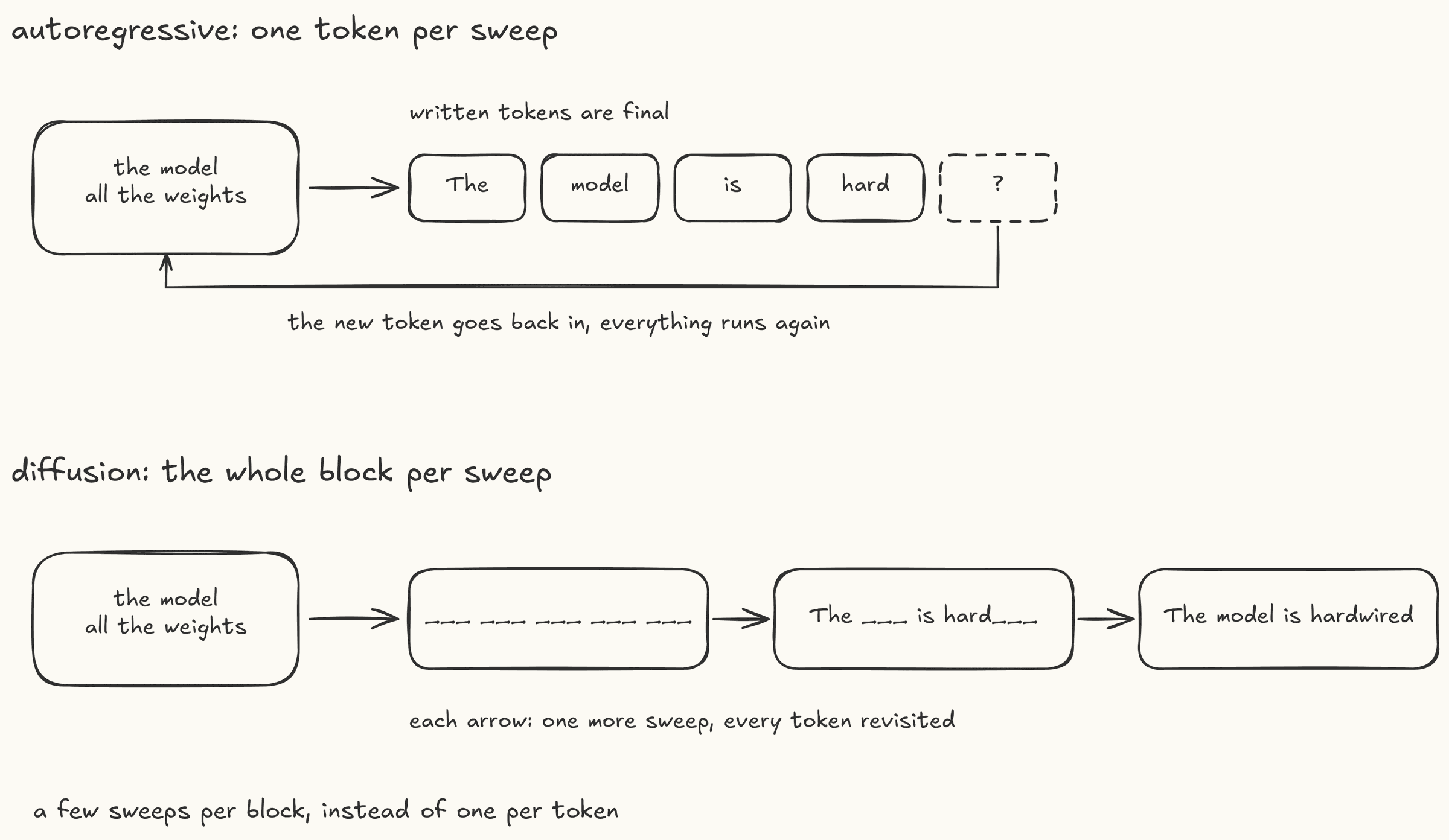
これはチップが行う取引と同じで、ソフトウェア版です。拡散モデルは、トークンごとに一度だけ重みを参照するのではなく、ブロックに対して複数のパスをかける余分な計算を行います。これにより、重みの再取得を防ぎます。GPU ではこの計算コストはほぼゼロです。単一ストリームのデコード中、演算ユニットはメモリの読み込み待ちでアイドル状態になっているからです。タラスとグロックがそれぞれチップ設計に費やした正是に、こうしたアイドル状態のシリコンを埋める非効率性を排除することでした。
計算リソースの追加は、単に速度を上げるだけではありません。自己回帰モデルは一度出力した単語を取り消すことができません。トークンが生成されると、その後のすべての処理に影響を与えるため、後続の部分で矛盾を生じさせることしかできないのです。一方、拡散モデルは生成過程全体を通じて同じ位置を繰り返し参照します。これが Google が「生成中にエラーを修正し、一貫性のある出力を実現する」と主張する理由です。
推論モデルも同様の目標を追っていますが、アプローチが逆です。既存のトークンを遡って修正するのではなく、より多くのトークンを追加することで回答を改善していきます。
より良い回答を得るためのあらゆる道筋には、提供されるトークンごとに計算リソースが必要となる。
つまり、期待した通りには計算が合わないのです。Groq は拡散モデル向けに再コンパイルして重みをローカルに集約できますが、Taalas はそれを刻印する必要があり、その計算能力は「1 つの刻印された重みあたり 1 倍」という物理的な制約があります。そのため、トークンあたりのパス数を増やすのは全く逆方向への動きになってしまいます。拡散モデルから最も恩恵を受けるハードウェアは、本来この作業を任されるはずだった GPU です。私はここでアーキテクチャに基づいて推論していますが、両方のチップに関する拡散モデルの実績データはまだ公開されていません。
市場の目にはこれは「黒馬」ですが、私の見方では本命です。まだ数字が私を裏付けているわけではありません。GPQA Diamond では Gemini Diffusion が Gemini 2.0 Flash-Lite に後れを取り(40.4% 対 56.5%)、Global MMLU でも同様に劣っています(69.1% 対 79.0%)。しかし、勝つ必要はありません。重要なのは、それを排除するために作られたものよりも、逐次的なボトルネックを小さくできるかどうかです。
すべてのものが互いに動き出すまで待たない
これが現在の議論の骨子ですが、今日という日自体が特別なのではありません。何が凍結され、何が読み込み可能になるかの境界線は自然に与えられるものではなく、設計上の判断です。その境界線の両側はいまだに設計段階にあります。
ハードウェアはすでに曲がり始めています。HC1 は独自仕様の 3 ビット形式を採用し、一部に 6 ビットの重みを混合した、そのモデル専用のエンコーディングに対応する専用チップでした。一方、HC2 では MXFP4 という業界標準の 4 ビットフォーマットへ移行しました。つまり、シリコンがモデルに合わせて適応しているのです。逆に、モデルをハードウェアに合わせる必要はもうありません。
ダイ上の SRAM の割合を半分増やせば、アダプタ容量が増え、同じベースモデルでより長いコンテキストを扱えるようになります。
モデル側も変化できます。最も明白な選択肢が「エキスパートの混合(Mixture-of-Experts)」です。各トークンを多数あるエキスパートのうち数個にルーティングするモデルは、ハードウェアが好むようなモジュール構造を持っています。頻繁にアクセスされるエキスパートをエッチングで固定し、長尾側の負荷はロード可能にする設計も可能です。あるいは、意図的に安定したトランク(幹)を持ち、上部を交換可能なモデルを設計することもできるでしょう。
これを実装した企業はまだありませんが、これは私の推測です。しかし、待機しているチップがあれば、こうした構造が作られるのは自然な流れです。
どちらの陣営も「ダークホース」に対応した製品を作ることができます。ブロック並列生成を最初から想定して設計されたチップは、別の種類のチップであり、不可能なわけではありません。重要なのはハードウェアかソフトウェアかの勝敗ではなく、これらがどこで収束し、最適な道が何になるかです。
ハードワイリングがその場所を得る理由
これらの動向は、Taalas への賭けが間違っていることを意味するものではありません。それは「狭い」賭けだということです。しかし、「狭い」ということは、決して侮蔑を意味しません。
本当に完成した機能は、地味なものです。音声認識、翻訳、OCR(光学文字認識)、検索用のテキスト埋め込み、コンテンツモデレーションなどです。これらはすでに小規模の専用モデルとして稼働しており、その処理量はマスクセットのコストを簡単に回収できるレベルに達しています。また、これらのモデルに対して求められる要件はここ数年ほとんど変わっていません。誰がOCR の人格アップデートを求めようとするでしょうか。
ディフュージョン(拡散)モデルもこれらを脅かすものではありません。テキスト埋め込みはそもそも単語単位で生成されるものではなく、モデレーション分類器の動作にも逐次的なボトルネックは存在しません。
Taalas はすでに 24 人のチームと 3000 万ドルの資金で最初のシリコン製品を完成させました。つまり、この分野がデータセンターを持つ企業に独占されているわけではありません。物理的な特性も小規模モデルに有利に働きます。8B パラメータのモデルなら単一のチップに収まりますが、1 トリオンパラメータの超大規模モデルでは、次世代チップを約 50 枚直列に接続する必要があります。
私は依然として、この技術の多くは小規模な専用モデルに集約されると考えています。そして、実際に金属(ハードウェア)として実装する価値があるのは、対話型の大規模モデルではなく、最もニッチで特化したモデルたちです。
So
モデルをシリコンに実装することは、そのモデルがどれほど長く静止し続けられるかという賭けです。SHA-256 の場合、この賭けは無料でした。なぜなら答えは永遠だからです。H.265 の場合は標準化作業に 10 年かかりました。そして 2026 年の汎用 LLM においては、19 ヶ月前の重みが、マスク代を取り戻すのに必要な 1 年間を凌駕するほど十分であるという賭けです。ただし、その賭けはアクセントだけを変えられ、思考を変えることはできない SRAM の帯によって一部ヘッジされています。
Taalas はおそらく狭い機能領域においてこの賭けに勝つでしょう。しかし広範な領域では、Groq が「そんなものは作らない」と拒否することで勝利する可能性が高いです。あるいは、今日モデルと今日のシリコンを用いて、そのどちらかに似た誰かが勝つかもしれません。ただし、Nvidia の Groq への 200 億ドル投資も、AMD の Taalas 買収も、「推論における高コストの要因はトークンごとに重みをフェッチすることにある」という前提に基づいています。そしてその前提を誤る最も安価な方法は、モデルがトークンを逐次生成するのをやめることです。しかし、どちらの買い手も、このリスクに対するヘッジを購入してはいません。
原文を表示
I first read about Taalas in February, in a Hacker News thread I opened expecting another inference startup with a benchmark chart. Instead it was a Toronto company that had taken Llama 3.1 8B and etched it into silicon - not loaded it, etched it, the weights laid down as physical transistors at the fab.
My first thought wasn't that this was new, it was that we've done this before. Groq had been working the same problem for years and stopped one step short, keeping the weights on the chip but still rewritable. The same question sits under both: how much of a model are you willing to make permanent in exchange for speed? Inside eight months, Nvidia had taken one of them and AMD the other.
That's the part worth paying attention to. Something quite significant is happening behind the curtains right about now, and it's easy to miss because it reads as chip news. Every previous time a workload left general-purpose hardware, it permanently changed who could afford to run it, and AI inference is somewhere in the middle of the same move. How far it goes isn't a fixed quantity waiting to be measured, because every part of the problem is still being designed - the models, the silicon, and, as it turns out, the way a model produces output at all.
We've seen this movie
Bitcoin mining went from CPUs to GPUs to FPGAs to purpose-built ASICs - application-specific integrated circuits, chips that do one job and nothing else - in four years. Each step traded flexibility for efficiency, and each was irreversible. When the first Avalon units shipped in 2013, GPU mining didn't get slower, it got pointless.
The pattern is everywhere now, and invisible precisely because it worked. YouTube transcodes video on its own Argos chips, which Google says beat its previous optimized software setup by 20 to 33 times. Network switching is Broadcom silicon. Your phone has a fixed-function block for H.265 decode, an ISP (image signal processor) for the camera, a Secure Enclave that does nothing else. It's what happens when a workload settles down enough to be worth casting in metal - and that condition is where this whole story ends up.
The wall they're all attacking
The thing GPUs spend most of their energy on during inference isn't math, it's moving weights. Every layer, every token, the weights come out of HBM (high-bandwidth memory, the stacked DRAM beside the GPU die) and through the compute units, then the next layer's follow. A 32-layer model does that 32 times to produce a single token, then starts over for the next. That's the memory wall - inference is limited by bandwidth, not compute, and HBM is the most expensive component on an AI server.
A chip that holds its weights on-die needs no HBM at all. Its memory is SRAM, printed on the logic wafer at a fab that isn't one of the memory plants whose 2027 output is already sold - so pushing inference onto this kind of silicon spreads the manufacturing load onto capacity that isn't already spoken for, and takes some pressure off the RAM and VRAM the rest of us are trying to buy. How much pressure is the open part, since the GPUs these chips get paired with still carry HBM.
Two companies have built exactly that, and they part ways on *how much of the model they were willing to freeze to do it*. Everything else follows from that.
Bet one: the model is the silicon
Taalas puts the weights in a mask-ROM fabric - read-only memory, written once during manufacture - where a single transistor stores four bits *and* performs the multiply related to it. Data flows through the chip's physical layers in sequence and never goes back out to external memory.
The numbers, all vendor-run and none independently verified:
- 16,960 tokens/second per user on Llama 3.1 8B, against roughly 230 on an H200. People who hit the public demo reported 14,000-17,000.
- 0.015 J/token, against Groq's self-reported 1-3 and roughly 10-30 for H100-class systems, per EE Times.
- $0.0075 per million tokens, against a typical $0.20-0.50.
- 815 mm² on TSMC N6, 53 billion transistors, about 250 W per card. One chip holds the whole 8B model.
"Etched in silicon" sounds like the chip is fixed the moment it leaves the fab. That's how most of the coverage reads, and how I read it at first, but it isn't quite true. The die has two regions. The mask-ROM fabric holds the frozen weights. Beside it sits an SRAM recall fabric - rewritable memory on the same chip - holding the KV cache and LoRA adapters, small sets of extra weights that steer a model toward a domain without retraining it. Those swap while the chip runs: the legal adapter gives you legal language, the clinical one medical, same etched model underneath.
Nor is the frozen half a full redesign. A chip is built from a stack of patterned layers, each printed through its own photomask, and cutting that mask set is the expensive part - tooling paid for before a single wafer moves. Taalas reuses the same base stack every time, with only two of the roughly hundred layers carrying the weights. It quotes about two months from new weights to shipping cards, where a full custom design runs six or more. Cost is harder to pin down, since published mask prices vary by an order of magnitude. The most specific estimate anyone has put on Taalas itself is zach.be's: about 30 chip variants and $100M in masks for a DeepSeek-R1-class model, so roughly $3M per variant, needing a year of service life to pay back.
So it's a spectrum, not a binary, and $3M is a line item for anyone already serving inference at scale. But it is still silicon. Two months is design time, not delivery time - Taalas had already slipped its own schedule by a year, and fabrication, validation and swapping cards out of racks come after it. And the adapters steer the hardwired weights rather than replacing them, so the chip picks up your terminology but not a capability the etched model never had. A revised base model, a different tokenizer or a new architecture means new masks and new cards.
Bet two: the model is loadable
Groq attacked the same wall from the other side, and the more I look at both, the more I think the hedge is the interesting part. The LPU (language processing unit) also has no HBM. Weights live in on-chip SRAM, placed by a compiler that works out every instruction and data movement in advance, so nothing is decided at runtime and latency is known before a job starts. Any model can run on it, and switching takes a recompile and a reload - minutes, no new hardware.
What that costs is capacity. First-generation LPUs carry 230 MB of SRAM per chip, which won't hold even a 7B model at 8-bit, and a 70B model spans 576 chips - interconnect, power and floor space for every one. The LP30 die improves the ratio without changing the problem, at roughly 500 MB, 256 to a rack for about 128 GB of on-chip SRAM. Still hundreds of chips to hold what Taalas fits on one die.
What they're actually betting on
Taalas bets the weights freeze - that a model stays useful long enough to earn back its masks, which its own economics put at about a year. Groq bets only the architecture freezes - transformers stay transformers, while the weights inside them keep changing every few months. Taalas is expensive in silicon per model. Groq is expensive in silicon per change of model.
Both bets have been endorsed with money. Nvidia licensed Groq's architecture for $20 billion in December, and AMD agreed to acquire Taalas just over seven months later - hedges against their own product being the wrong shape for most of the work. More interesting than either deal is that both buyers described the same system design. Answering a prompt has two phases: reading the input, which is parallel math and exactly what a GPU is good at, and writing the reply one word at a time, each word needing the whole model again before the next can start. Both put the GPU on the first phase and the specialized chip on the second. Two opposite philosophies about what to freeze, one identical division of labour.
Where the analogy breaks
Bitcoin got its ASICs because SHA-256 is a specification, standardized in 2002, years before Bitcoin existed. It will never change - not "probably won't" but *can't*, because changing it would be a different currency. Video codecs went the same way: standardize the format, wait, then put it in silicon.
The precondition was never "this workload is popular." It was "this workload is finished."
LLMs are pretty fluid tools, and I don't think they're anywhere near finished. Llama 3.1 8B came out in July 2024, so HC1 shipped in February 2026 baking a nineteen-month-old model, with better ones already out in its size class. Silicon takes long enough to arrive holding something the world has moved past.
The usual counter is that the pace will settle. I half agree. The *breakthroughs* do look like they're slowing - the transformer has held for nine years, mixture-of-experts is standard, genuinely new architectural ideas arrive further apart. But releases won't slow much, and releases are what breaks the chip. Llama 3.1 to 3.2 to 3.3, Qwen 2.5 to 3, a post-training refresh, a tokenizer swap. Every one keeps the architecture identical and changes the numbers, and the numbers are what was cast in metal.
And most customers need flexibility first of all. Ask a phone assistant "what's this charge on my bill?" and it runs speech recognition, a vision model on the screenshot, a language model to reason about it, then speech synthesis - four models, three modalities, one question, and the mix shifts as better ones arrive. A chip that does one of those extremely fast and none of the others solves very little.
The dark horse nobody is buying
Every argument so far leaves one assumption standing: a model writes one word at a time. Both designs are built on it. But nothing forces a model to.
Diffusion language models don't. Google's Gemini Diffusion "generates entire blocks of tokens at once," refining a whole rough draft in place rather than extending a sentence, and reports 1,479 tokens per second of sampling. One sweep of the weights per block instead of one per word. Google publishes neither the model's size nor the hardware it ran on, so that figure won't line up against the ones above, and the demo is invite-only. The one you can put a prompt into today is Inception's Mercury, selling the same idea as a product - by its own claim, 5 to 7 times the throughput at 70% lower cost per task.
That's the same trade the chips make, only in software. Diffusion spends extra arithmetic - several passes over a block rather than one pass per token - to avoid re-fetching weights. On a GPU that arithmetic is nearly free, because during single-stream decode the compute units sit idle waiting on memory. Filling idle silicon is precisely the inefficiency Taalas and Groq spent a chip design each to remove.
That extra arithmetic buys more than speed. An autoregressive model cannot unsay a word - once a token is out it conditions everything that follows, and the best the model can do is contradict itself further down the page. A diffusion model revisits the same positions across sweeps, which is why Google claims it "corrects errors during generation for more consistent outputs." Reasoning models chase the same thing from the opposite direction, improving an answer by generating more tokens rather than by going back over the ones they have. Every route to a better answer costs compute per delivered token.
So the two don't add up the way you'd hope. Groq can recompile for a diffusion model and collect little, its weights being local already. Taalas would have to etch one, and its compute is physically fixed at one multiplier per etched weight, so more passes per token runs the wrong way entirely. The hardware that gains most from diffusion is the GPU that was supposed to hand the job off. I'm reasoning from the architectures here - nobody has published diffusion numbers on either chip.
It's a dark horse in the market's eyes and a favourite in mine. The numbers don't back me up yet: Gemini Diffusion still trails Gemini 2.0 Flash-Lite on GPQA Diamond, 40.4% against 56.5%, and on Global MMLU, 69.1% against 79.0%. But it doesn't have to win. It only has to make the sequential bottleneck smaller than the thing built to remove it.
Unless everything moves toward everything else
That's the argument as it stands today, and today is not the interesting part. The line between what gets frozen and what stays loadable isn't handed down by nature. It's a design decision, and every side of it is still being designed.
Hardware is already bending. HC1 used a proprietary 3-bit format with some 6-bit weights mixed in - a bespoke chip for a bespoke encoding. HC2 moves to MXFP4, an industry-standard 4-bit format, so the silicon is adapting to what models already do rather than the other way round. Give the SRAM half a bigger share of the die and you buy more adapter capacity and longer context on the same frozen base.
Models can move too, and mixture-of-experts is the obvious opening. A model that routes each token through a few of many experts is already modular in the way silicon likes. Nothing stops someone etching the experts that get hit constantly and leaving the long tail loadable, or designing a model with a deliberately stable trunk and a replaceable top. Nobody has shipped this - I'm speculating - but it's the sort of thing that gets built when there's a chip waiting for it.
And either camp can build for the dark horse. A chip designed from the start for block-parallel generation is a different chip, not an impossible one. The question was never whether hardware or software wins. It's where all of this converges, and what the optimal path turns out to be.
Where hardwiring does earn its place
None of this makes the Taalas bet a bad one. It makes it a *narrow* one, and narrow isn't an insult.
The functions that are genuinely finished are the boring ones. Speech recognition. Translation. OCR. Text embeddings for retrieval. Content moderation. These already run as small dedicated models, at volumes that would pay off a mask set easily, and what we ask of them has barely moved in years. Nobody is going to demand a personality update for their OCR. Diffusion doesn't threaten them either. Text embeddings aren't produced a word at a time in the first place, and nothing about a moderation classifier is waiting on the sequential bottleneck.
Taalas got first silicon out with 24 people and $30 million, so this isn't structurally reserved for people who own datacenters. The physics rewards small directly too: an 8B model fits on one die, a trillion-parameter one needs about fifty of the next-generation chips wired in sequence. I still think small dedicated models are where most of this ends up, and the ones worth casting in metal are the narrowest, not the ones you talk to.
So
Casting a model into silicon is a bet on how long it can stand still. For SHA-256 the bet was free, because the answer is forever. For H.265 it cost a decade of standards work. For a general-purpose LLM in 2026, it's a bet that a nineteen-month-old set of weights is close enough for the year it takes to earn the masks back - hedged by a strip of SRAM that lets you change its accent but not its mind.
Taalas will probably win that bet on a narrow function. On the broad one, Groq is likely to win by refusing to make it - on today's models, with today's silicon. Or somebody shaped like either of them. But Nvidia's $20 billion on Groq and AMD's purchase of Taalas both went to the premise that the expensive part of inference is fetching weights one token at a time, and the cheapest way to be wrong about that is for the models to stop writing one token at a time. Neither buyer has bought a hedge against that one.
関連記事
News to Guide
ニュースの次に確認する
発表内容を、現在の料金や仕様と照らし合わせられる関連ガイドです。
今日のまとめ
AIデイリーブリーフで今日の重要ニュースをまとめ読み